There is a moment every product designer remembers. You are staring at a board layout that simply will not fit. The components keep multiplying, the connections keep tangling, and the case you designed last month suddenly feels two sizes too small. If you have felt that frustration, you are not alone, and more importantly, you are not stuck.
It usually starts the same way. A product that looked spacious on paper turns into a tight, frustrating puzzle the moment real components enter the picture. Connectors need room, antennas need clearance, batteries need their own footprint, and somehow the circuit board is expected to shrink around all of it without losing a single function. The good news is that this is rarely a sign of a bad design. It is usually a sign that the board technology has not caught up with the ambition behind the product yet.
When Space Becomes the Enemy of Good Design
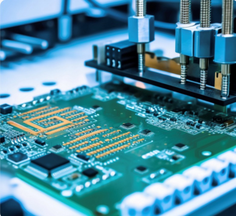
This is exactly the kind of problem that High Density Interconnect technology was built to solve. An hdi pcb manufacturer uses blind vias, buried vias, and laser drilled microvias to pack more routing into less space than you ever thought possible. Instead of fighting your enclosure, your board finally works with it. Here is what that actually means once it reaches your design:
- Smaller footprint: microvias and buried vias can shrink your board area by more than thirty percent, the difference between a wearable that feels clunky and one that feels effortless on the wrist
- Cleaner high speed signals: shorter traces and tightly controlled impedance support differential rates as high as 28 Gbps, so signals stay clean instead of getting lost in noise
- Stacking freedom: layer counts ranging from four to thirty two mean your design team stops compromising and starts creating
The Quiet Wins Nobody Talks About
There is also a quieter benefit that engineers come to appreciate over time. Shorter return paths and a more even layer distribution reduce EMI and EMC issues before they ever become a certification headache. That means fewer late nights chasing interference problems and fewer surprises when your product reaches compliance testing.
None of this happens by accident. It comes down to process control that most people never see:
- Laser micro vias as small as 0.10 mm with smooth, consistent walls
- Sequential lamination with temperature control held within two degrees
- Via fill processes that keep planarity under ten microns
These are not abstract numbers on a spec sheet. A board that looks fine under a microscope can still fail in the field if a single via has an uneven copper deposit or if lamination pressure drifted by even a fraction during the press cycle. Process discipline at this level is not glamorous, but it is the difference between a product that earns trust and one that generates support tickets.
Where This Technology Actually Belongs
If you are building for any of the following, HDI is the foundation your project is standing on:
- 5G infrastructure and antenna modules
- Automotive electronics and ADAS systems
- Medical devices and wearable health monitors
- Industrial automation and IoT controllers
- Aerospace and defense electronics
Get it right, and everything downstream becomes easier. Get it wrong, and you spend months firefighting issues that should never have existed.
So here is the honest question worth asking yourself today. Are you still designing around the limitations of your board, or are you ready to let your board catch up to your imagination? When you are ready to see what a tighter, faster, smarter layout could do for your product, take a look at Fast Turn PCB. Built in 2015 to solve the industry biggest pain point, long lead times, the company now runs a technology driven production system that combines automated quoting with 24 hour turnaround and delivery in as little as 24 to 36 hours, all backed by 15 years of hands on PCB and PCBA experience. First time customers can even claim 25 percent off their opening order. Fast Turn PCB works through these layout decisions with engineers every day, and sometimes the smallest board change is the one that finally lets your big idea breathe.